 | ÐлекÑÑоннÑй компоненÑ: LTC1325CN | СкаÑаÑÑ:  PDF PDF  ZIP ZIP |
Äîêóìåíòàöèÿ è îïèñàíèÿ www.docs.chipfind.ru
1
LTC1325
Microprocessor-Controlled
Battery Management System
FEATURES
DESCRIPTIO
N
U
s
Fast Charge Nickel-Cadmium, Nickel-Metal-Hydride,
Lithium Ion or Lead-Acid Batteries under
µ
P Control
s
Flexible Current Regulation:
Programmable 111kHz PWM Current Regulator
with Built-In PFET Driver
PFET Current Gating for Use with External Current
Regulator or Current Limited Transformer
s
Discharge Mode
s
Measures Battery Voltage, Battery Temperature and
Ambient Temperature with Internal 10-Bit ADC
s
Battery Voltage, Temperature and Charge Time
Fault Protection
s
Built-In Voltage Regulator and Programmable
Battery Attenuator
s
Easy-to-Use 3- or 4-Wire Serial
µ
P Interface
s
Accurate Gas Gauge Function
s
Wide Supply Range: V
DD
= 4.5V to 16V
s
Can Charge Batteries with Voltages Greater Than V
DD
s
Can Charge Batteries from Charging Supplies Greater
Than V
DD
s
Digital Input Pins Are High Impedance in
Shutdown Mode
The LTC
®
1325 provides the core of a flexible, cost-effec-
tive solution for an integrated battery management sys-
tem. The monolithic CMOS chip controls the fast charging
of nickel-cadmium, nickel-metal-hydride, lead-acid or
lithium batteries under microprocessor control. The de-
vice features a programmable 111kHz PWM constant
current source controller with built-in FET driver, 10-bit
ADC, internal voltage regulator, discharge-before-charge
controller, programmable battery voltage attenuator and
an easy-to-use serial interface.
The chip may operate in one of five modes: power shut-
down, idle, discharge, charge or gas gauge. In power
shutdown the supply current drops to 30
µ
A and in the idle
mode, an ADC reading may be made without any switching
noise affecting the accuracy of the measurement. In the
discharge mode, the battery is discharged by an external
transistor while the battery is being monitored by the
LTC1325 for fault conditions. The charge mode is termi-
nated by the
µ
P while monitoring any combination of
battery voltage and temperature, ambient temperature
and charge time. The LTC1325 also monitors the battery
for fault conditions before and during charging. In the gas
gauge mode the LTC1325 allows the total charge leaving
the battery to be calculated.
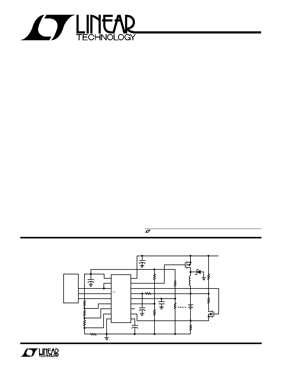
s
System Integrated Battery Charger
APPLICATIO
N
S
U
TYPICAL APPLICATIO
N
U
, LTC and LT are registered trademarks of Linear Technology Corporation.
Battery Charger for up to 8 NiCd or NiMH Cells
1
2
3
4
5
6
7
8
9
18
17
16
15
14
13
12
11
10
V
DD
PGATE
DIS
V
BAT
T
BAT
T
AMB
V
IN
SENSE
FILTER
LTC1325
REG
D
OUT
D
IN
CS
CLK
LTF
MCV
HTF
GND
+
R1
C
REG
4.7
µ
F
THERM 2
THERM 1
R5
R
DIS
R
TRK
R
SENSE
LTC1325 · TA01
L1
62
µ
H
BAT
N1
IRFZ34
V
DD
4.5V TO 16V
R13
R2
R3
R4
C
F
1
µ
F
MPU
(e.g. 8051)
p1.4
p1.3
p1.2
+
C2
10
µ
F
+
C
REG
22
µ
F
C1
0.1
µ
F
100
D1
1N6818
P1
IRF9730
2
LTC1325
SYMBOL
PARAMETER
CONDITIONS
MIN
TYP
MAX
UNITS
V
DD
V
DD
Supply Voltage
q
4.5
16
V
I
DD
V
DD
Supply Current
All TTL Inputs = 0V or 5V, No Load on REG
q
1200
2000
µ
A
I
PD
V
DD
Supply Current
Power-Down Mode, All TTL Inputs = 0V or 5V
q
30
50
µ
A
V
REG
Regulator Output Voltage
No Load
q
3.047
3.072
3.097
V
LD
REG
Regulator Load Regulation
Sourcing Only, I
REG
= 0mA to 2mA
1
5
mV/mA
LI
REG
Regulator Line Regulation
No Load, V
DD
= 4.5V to 16V
60
100
µ
V/V
TC
REG
Regulator Output Tempco
No Load, 0
°
C < T
A
< 70
°
C
50
ppm/
°
C
V
DAC
DAC
Output Voltage
VR1 = 1, VR0 = 1, 100% Duty Ratio, I
CHRG
= I (Note 7)
140
160
180
mV
VR1 = 1, VR0 = 0, 100% Duty Ratio, I
CHRG
= I/3
48
55
62
mV
VR1 = 0, VR0 = 1, 100% Duty Ratio, I
CHRG
= I/5
30
34
38
mV
VR1 = 0, VR0 = 0, 100% Duty Ratio, I
CHRG
= I/10
16
18
21
mV
V
HYST
Fault Comparator Hysteresis
V
HTF
= 1V, V
EDV
= 0.9V, V
BATR
= 100mV
±
20
mV
V
MCV
= V
LTF
= 2V
±
10
mV
V
OS
Fault Comparator Offset
V
HTF
= 1V, V
EDV
= 0.9V, V
BATR
= 100mV
±
50
mV
V
MCV
= V
LTF
= 2V
V
BATR
V
BAT
for BATR = 1
100
mV
V
BATP
V
BAT
for BATP = 1
q
V
DD
1.8
V
V
EDV
Internal EDV Voltage
q
860
900
945
mV
V
LTF
, V
MCV
LTF, MCV Voltage Range
1.6
2.8
V
V
HTF
HTF Voltage Range
0.5
1.3
V
A
GG
Gas Gauge Gain
0.4V < V
SENSE
< 0V
4
V
OS(GG)
Gas Gauge Offset
0.4V < V
SENSE
< 0V (Note 6)
±
1
LSB
R
F
Internal Filter Resistor
1000
TOL
BATD
Battery Divider Tolerance
All Division Ratios
q
2
2
%
V
IL
Input Low Voltage
CLK, CS, D
IN
q
0.8
1.3
V
V
IH
Input High Voltage
CLK, CS, D
IN
q
1.7
2.4
V
I
IL
Low Level Input Current
V
CLK
, V
CS
or V
DIN
= 0V
q
2.5
2.5
µ
A
I
IH
High Level Input Current
V
CLK
, V
CS
or V
DIN
= 5V
q
2.5
2.5
µ
A
ELECTRICAL CHARACTERISTICS
ORDER PART
NUMBER
ABSOLUTE
M
AXI
M
U
M
RATINGS
W
W
W
U
PACKAGE/ORDER I
N
FOR
M
ATIO
N
W
U
U
Consult factory for Industrial and Military grade parts.
V
DD
= 12V
±
5%, T
A
= 25
°
C, unless otherwise noted.
(Notes 1, 2)
V
DD
to GND ............................................................. 17V
All Other Pins ................................ 0.3V to V
DD
+ 0.3V
Operating Temperature Range ..................... 0
°
C to 70
°
C
Storage Temperature Range ................. 65
°
C to 150
°
C
Lead Temperature (Soldering, 10 sec).................. 300
°
C
1
2
3
4
5
6
7
8
9
TOP VIEW
N PACKAGE
18-LEAD PDIP
18
17
16
15
14
13
12
11
10
REG
D
OUT
D
IN
CS
CLK
LTF
MCV
HTF
GND
V
DD
PGATE
DIS
V
BAT
T
BAT
T
AMB
V
IN
SENSE
FILTER
SW PACKAGE
18-LEAD PLASTIC SO WIDE
T
JMAX
= 125
°
C,
JA
= 75
°
C/ W (N)
T
JMAX
= 125
°
C,
JA
= 100
°
C/ W (SW)
LTC1325CN
LTC1325CSW
3
LTC1325
V
DD
= 12V
±
5%, T
A
= 25
°
C, unless otherwise noted.
ELECTRICAL CHARACTERISTICS
SYMBOL
PARAMETER
CONDITIONS
MIN
TYP
MAX
UNITS
t
hDI
Hold Time, D
IN
After CLK
150
ns
t
dsuCS
Setup Time, CS Before First CLK
1
µ
s
t
dsuDI
Setup Time, D
IN
Stable Before First CLK
400
ns
t
WHCLK
CLK High Time
0.8
µ
s
t
WLCLK
CLK Low Time
1
µ
s
t
WHCS
CS High Time Between Data Transfers
1
µ
s
t
WLCS
CS Low Time During Data Transfer
MSBF = 1
43
CLK Cycles
MSBF = 0
52
CLK Cycles
RECO E
DED CHARACTERISTICS
UW
W
The
q
denotes specifications which apply over the full operating
temperature range.
Note 1: Absolute Maximum Ratings are those values beyond which the life
of a device may be impaired.
Note 2: All voltage values are with respect to the GND pin.
Note 3: V
REG
within specified min and max limits, CLK (Pin 5) = 500kHz,
unless otherwise stated. ADC clock is the serial CLK.
Note 4: Linearity error is specified between the actual end points of the
A/D transfer curve.
Note 5: Channel leakage is measured after channel selection.
Note 6: Gas gauge offset excludes A/D offset error.
Note 7: I = V
DAC
(Duty Ratio)/R
SENSE
, where V
DAC
is the DAC output
voltage with control bits VR1 = VR0 = 1, duty ratio = 1 and R
SENSE
is
determined by the user.
SYMBOL
PARAMETER
CONDITIONS
MIN
TYP
MAX
UNITS
V
OL
Output Low Voltage
D
OUT
, I
OUT
= 1.6mA
q
0.4
V
V
OH
Output High Voltage
D
OUT
, I
OUT
= 1.6mA
q
2.4
V
I
OZ
Hi-Z Output Leakage
V
CS
= 5V
q
±
10
µ
A
V
OHFET
DIS or PGATE Output High
V
DD
= 4.5V to 16V
q
V
DD
0.05
V
V
OLFET
DIS or PGATE Output Low
V
DD
= 4.5V to 16V
q
0.05
V
t
dDO
Delay Time, CLK
to D
OUT
Valid
See Test Circuits
q
650
ns
t
dis
Delay Time, CS
to D
OUT
Hi-Z
See Test Circuits
q
510
ns
t
en
Delay Time, CLK
to D
OUT
Enabled
See Test Circuits
q
400
ns
t
hDO
Time D
OUT
Remains Valid After CLK
See Test Circuits
q
30
ns
t
rDOUT
D
OUT
Rise Time
See Test Circuits
q
250
ns
t
fDOUT
D
OUT
Fall Time
See Test Circuits
q
100
ns
f
CLK
Serial I/O Clock Frequency
CLK Pin
q
25
500
kHz
t
rPGATE
PGATE Rise Time
C
LOAD
= 1500pF
q
150
ns
t
fPGATE
PGATE Fall Time
C
LOAD
= 1500pF
q
150
ns
f
OSC
Internal Oscillator Frequency
Charge Mode, Fail-Safes Disabled
90
111
130
kHz
A/D Converter
Offset Error
V
IN
Channel (Note 3)
q
±
2
LSB
Linearity Error
V
IN
Channel (Notes 3, 4)
q
±
0.5
LSB
Full-Scale Error
V
IN
Channel (Note 3)
q
±
1
LSB
On-Channel Leakage
V
IN
Channel ON Only (Notes 3, 5)
q
±
10
µ
A
Off-Channel Leakage
V
IN
Channel OFF (Notes 3, 5)
q
±
10
µ
A
4
LTC1325
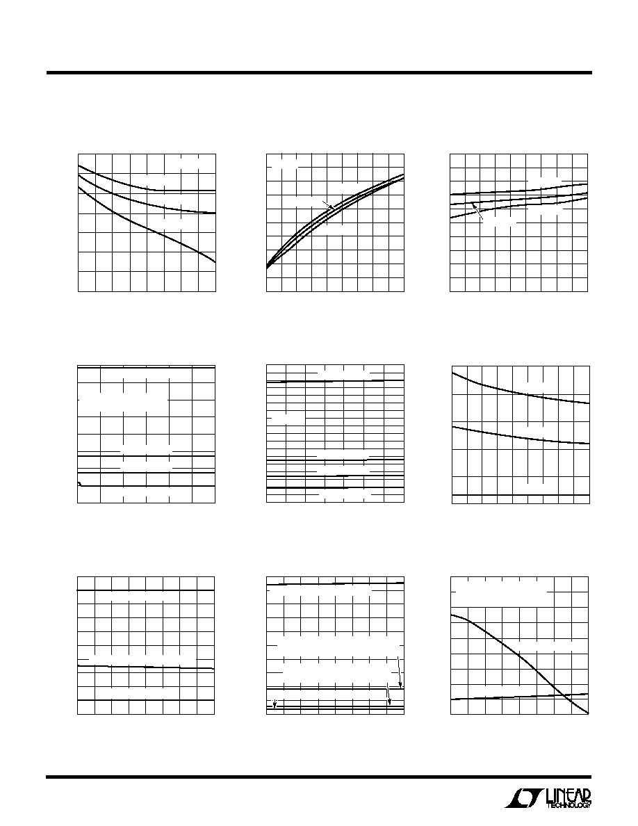
TYPICAL PERFOR
M
A
N
CE CHARACTERISTICS
U
W
LOAD CURRENT
(mA)
0
REGULATOR OUTPUT VOLTAGE (V)
3.074
3.075
3.076
3.0
1325 G01
3.073
3.072
0.5
1.0
1.5
2.5
3.5
2.0
4.0
3.071
3.070
3.077
V
DD
= 12V
V
DD
= 4.5V
V
DD
= 16V
T
A
= 27
°
C
TEMPERATURE (
°
C)
0
0
SHUTDOWN CURRENT (
µ
A)
5
15
20
25
20
40
50
90
1325 G06
10
10
30
60
70
80
V
DD
= 12V
V
DD
= 16V
V
DD
= 4.5V
TEMPERATURE (
°
C)
0
V
DD
SUPPLY CURRENT (
µ
A)
1000
900
800
700
600
500
400
300
200
100
0
20
40
50
90
1325 G03
10
30
60
70
80
V
DD
= 16V
V
DD
= 4.5V
V
DD
= 12V
DAC Output Voltage vs
Temperature
TEMPERATURE (
°
C)
0
3.072
3.073
3.075
3.076
3.077
3.082
3.079
20
40
50
90
1325 G02
3.074
3.080
3.081
3.078
10
30
60
70
80
V
DD
= 16V
I
REG
= 0
V
DD
= 4.5V
REGULATOR OUTPUT VOLTAGE (V)
V
DD
= 12V
Fault Comparator Threshold vs
Temperature
Fault Comparator Threshold vs
Temperature
TEMPERATURE (
°
C)
0
FAULT COMPARATOR THRESHOLD (V)
11
10
9
8
7
6
5
4
3
2
1
20
40
50
1325 G08
10
30
60
70
80
V
BAT
FOR BATP = HIGH, V
DD
= 12V
V
CELL
FOR MCV = HIGH, V
MCV
= 2.8V AND
V
TBAT
FOR LTF = HIGH, V
LTF
= 2.8V
V
TBAT
FOR HTF = HIGH, V
HTF
= 1.35V
V
CELL
FOR MCV = HIGH, V
MCV
= 1.6V
V
TBAT
FOR LTF = HIGH, V
LTF
= 1.6V
Gas Gauge Gain and Offset vs
Temperature
V
DD
Supply Current vs
Temperature
TEMPERATURE (
°
C)
0
4.5
GAS GAUGE GAIN AND OFFSET (COUNTS)
4.0
3.0
2.5
2.0
70
60
0
1325 G09
3.5
10
20
30
40
50
80
1.5
1.0
0.5
V
SENSE
= 0.2V AND 0.4V
INCLUDES CHANGES IN V
REG
WITH TEMPERATURE
GAS GAUGE OFFSET
GAS GAUGE GAIN
Charge Current vs Battery Voltage
Regulator Output Voltage vs
Load Current
Regulator Output Voltage vs
Temperature
TEMPERATURE (
°
C)
0
DAC OUTPUT VOLTAGE (mV)
180
160
140
120
100
80
60
40
20
0
30
50
1325 G05
10
20
40
60
70
V
DD
= 12V
VR1 = 1, VR0 = 1
VR1 = 1, VR0 = 0
VR1 = 0, VR0 = 0
VR1 = 0, VR0 = 1
Shutdown Current vs Temperature
BATTERY VOLTAGE (V)
0
CHARGE CURRENT (mA)
160
140
120
100
80
60
40
20
0
2
4
6
8
1325 G04
10
12
VR1 = 1, VR0 = 1
VR1 = 1, VR0 = 0
VR1 = 0, VR0 = 0
VR1 = 0, VR0 = 1
V
DD
= 12V, R
SENSE
= 1
,
L = 100
µ
H, P1: IRF9531
TEMPERATURE (
°
C)
0
0
FAULT COMPARATOR THRESHOLD (V) 0.1
0.3
0.4
0.5
1.0
0.7
20
40
50
1325 G07
0.2
0.8
0.9
0.6
10
30
60
70
80
V
CELL
FOR EDV = HIGH
V
TBAT
FOR HTF = HIGH, V
HTF
= 0.4V
V
CELL
FOR BATR = HIGH
5
LTC1325
TYPICAL PERFOR
M
A
N
CE CHARACTERISTICS
U
W
LOAD CAPACITANCE (nF)
0
PGATE RISE TIME (ns)
400
800
1200
1000
600
200
4
8
12
16
1325 G10
20
2
0
6
10
14
18
T
A
= 0
°
C
T
A
= 70
°
C
T
A
= 27
°
C
LOAD CAPACITANCE
(nF)
0
PGATE FALL TIME (ns)
600
800
1000
900
700
500
300
100
16
LTC1325 G11
400
200
0
4
2
6
10
14
18
8
12
20
T
A
= 70
°
C
T
A
= 0
°
C
T
A
= 27
°
C
PGATE Fall Time vs
Load Capacitance
CODE
0
DIFFERENTIAL NONLINEARITY (LSB)
1024
1325 G12
256
512
768
1.0
0.5
0
0.5
1.0
128
384
640
896
V
DD
= 12V
f
CLK
= 500kHz
LOAD CAPACITANCE (nF)
0
0
DISCHARGE RISE AND FALL TIME (
µ
s)
2
6
8
10
14
2
10
14
1325 G13
4
12
8
18 20
4
6
12
16
T
A
= 70
°
C
T
A
= 27
°
C
T
A
= 0
°
C
RISE TIME
FALL TIME
CODE
0
INTEGRAL NONLINEARITY (LSB)
1024
1325 G15
256
512
768
1.0
0.5
0
0.5
1.0
128
384
640
896
V
DD
= 12V
f
CLK
= 500kHz
Integral Nonlinearity
TEMPERATURE (
°
C)
40
108
OSCILLATOR FREQUENCY (kHz)
109
111
112
113
118
115
0
40
60
1325 G16
110
116
117
114
20
20
80
100
Oscillator Frequency vs
Temperature
TEMPERATURE (
°
C)
0
CLK TO D
OUT
VALID DELAY TIME (ns)
400
500
600
60
1325 G18
300
200
10
20
30
50
70
40
80
100
0
700
D
OUT
GOING HIGH
D
OUT
GOING LOW
CLK to D
OUT
Enable Delay Time
vs Temperature
CLK to D
OUT
Valid Delay Time
vs Temperature
TEMPERATURE (
°
C)
0
0
CLK TO D
OUT
ENABLE DELAY TIME (ns)
50
150
200
250
500
350
20
40
50
1325 G17
100
400
450
300
10
30
60
70
80
NUMBER OF CELLS
1
MINIMUM CHARGE VOLTAGE (V)
7
1325 G14
3
5
16
14
12
10
8
6
4
2
0
2
4
6
8
R
SENSE
= 1, VR1 = 1, VR0 = 1
L = 25
µ
H TO 100
µ
H
IRF9Z30PFET, 1N5819 DIODE
R
SENSE
= 0.15, VR1 = 1,VR0 = 1
L = 10
µ
H TO 100
µ
H
IRF9Z30PFET, 1N5819 DIODE
T
A
= 27
°
C, NiCd BATTERIES
V
CELL
= 1.4V NOMINAL
Discharge Rise and Fall Time
vs Load Capacitance
Minimum Charging Supply vs
Number of Cells
Differential Nonlinearity
PGATE Rise Time vs
Load Capacitance